Microcomputer system includes processor, memory, interface, and modem
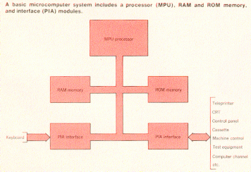 The MC6800, 8-bit microprocessor unit (MPU) is being made available with
supporting components including a 128-by-8-bit random access memory (RAM),
a 1024-by-8-bit read-only memory (ROM), a peripheral interface adapter (PIA),
and a single-chip 0-600 bps modem. All these components are TTL compatible,
MOS n-channel, silicon gate devices, and only a single, 5.0-volt supply is
needed for all the devices. The system uses a single bus organization that
allows memory and interface devices to share the same address space. All
MPU and system bus control functions are available on separate, TTL level pins,
and no multiplexing or decoding is required for operation: interfacing is
accomplished without additional TTL parts.
The MC6800, 8-bit microprocessor unit (MPU) is being made available with
supporting components including a 128-by-8-bit random access memory (RAM),
a 1024-by-8-bit read-only memory (ROM), a peripheral interface adapter (PIA),
and a single-chip 0-600 bps modem. All these components are TTL compatible,
MOS n-channel, silicon gate devices, and only a single, 5.0-volt supply is
needed for all the devices. The system uses a single bus organization that
allows memory and interface devices to share the same address space. All
MPU and system bus control functions are available on separate, TTL level pins,
and no multiplexing or decoding is required for operation: interfacing is
accomplished without additional TTL parts.
Arrangements have been made with American Microsystems Inc., Santa Clara, Calif., to second-source the M6800 MPU, PIA, RAM and ROM.
A 16-bit address bus provides the MC6800 with access to 65k bytes of memory. Three-state operation of the data and address line is permitted. When in the open (high-impedence) state, direct memory addressing is possible; this mode also provides a multiple processor capability.
The MPU will respond to a set of 72 variable-length instructions. This repertoire includes binary, two's complement, and decimal arithmetic, as well as shift, rotate, load, store, conditional or unconditional branch, interrupt, and stack-manupulation instructions. In addition, the MC6800 has seven address modes, and the type of coding of the instruction fetched will determine whether the address mode for that instruction is direct, relative, immediate, indexed, extended, implied, or accumulated. The MPU contains six program-available registers. The 2-byte registers (and their functions) are: program counter (points to the current program address); stack pointer (contains the address of the next available location in an external push-down/pop-up memory stack); index register (stores data or a 16-bit address for the indexed mode of memory addressing). The single-byte registers (and their functions) are: two accumulators (to hold operands and results from an internal arithmetic logic unit); and condition code register (contains the results of arthmetic logic operations and serves as a decision block for conditional branching).
Timing of the MPU is accomplished with a two-phase clock at rates of up to 1.0 MHz.
Operating statically, the n-channel, silicon gate MCM6810, 128-by-8-bit RAM does not need to be clocked or refreshed. Data flow in this byte-organized memory is bidrectional: the data buffers are three-state operable. Six chip select inputs provide a means of increasing the size of a memory subsystem without the need for additional decoding. Two versions of the RAM memory are available: the MCM6810L has a maximum access time of 1.0 microseconds, while the MCM6810L-1 version has a maximum access time of 600 nanoseconds.
The mask-programmable, MCM6830L, is a 1024-by-8-bit read-only memory. This byte-organized ROM is used to store the control programs for the MC6800 MPU; however, it may also be used in other bus-organized applications. The MCM-6830L operates in the static mode, eliminating the need for clock and refresh inputs. Four chip select inputs provide a means for memory expansion; these inputs may be specified as positive or negative enable, by the customer, during the mask-programming stage.
The MC6820 Peripheral Interface Adapter (PIA) provides a means of interfacing peripheral equipment to the MC6800 MPU. The PIA can be programmed during system initialization to perform specific input-output (I/O) management tasks. As a consequence, I/O control is distributed throughout the system bus, rather concentrated at the MPU. The result is a highly adaptive system configuration that can be used with a variety of peripherals.
Data transfer between the PIA and a peripheral device occurs on 16 I/O lines organized as two 8-bit bidirectional busses. Each I/O line may be individually programmed to act as either an input or output of the PIA. Input data are transferred directly to the MPU data bus; output data are latched in two PIA peripheral interface output registers. I/O programming is accomplished by means of two PIA data direction registers.
The MC6860L, single-chip digital modem, provides modulation, demodulation, and supervisory control functions necessary to implement a serial data communications link. Employing frequency shift keying (FSK) modulation, data at rates up to 600 bps can be transferred by means of a standard, voice-grade telephone channel. Modes of operation for the MC6860L include full duplex, half duplex, simplex, automatic answering, automatic disconnect, originate only, answer only, and answer/originate. The modem is TTL compatible.
The price of 40-pin, ceramic, dual-in-line package MC6800 MPU is $360. Prices for the 24-pin, ceramic, DIP RAMs are $30.50 for the MCM6810L, and $37.50 for the MCM6810L-1. For the MCM6830L ROM - in a 24-pin ceramic DIP - the price is $35. The MC6820 PIA costs $28 in a 40-pin ceramic DIP; and the MC6960L modem, in a 24-pin DIP, costs $75. All prices are for 1-24 quantities.
For further information, contact the Technical Information Center, Motorola Inc., Semiconductor Products Division, P.O. Box 20294, Phoenix, Ariz. 85036.