|
magnetic bubble memory description
Magnetic bubble memory technology has advanced considerably since the
concept was introduced by Bell Telephone Laboratories in 1967. Research
indicated that small cylindrical magnetic domains, which are called
magnetic bubbles, can be formed in single-crystal thin films of
synthetic ferrites or garnets when an external magnetic field is applied
perpendicularly to the surface of the film. These bubbles can be moved
laterally through the film by using a varying magnetic field. These
characteristics of magnetic bubles make them ideally suited for serial
storage of data bits; the
presence or absence of a bubble in a bit position is used to define the
logic state. Since the diameter of a bubble is so
small (as little as a tenth of a micrometer), many thousands of data
bits can be stored in a signle bubble-memory chip.
In the spring of 1977 Texas Instruments was the first to market a
92,304-bit bubble memory. This bubble memory is
much like magnetic tape or magnetic disc memory storage in that it is
nonvolatile meaning that the data is retained even when power is no
longer applied to the chip. Since bubble memories are a product of
solid-state technology
(there are no moving parts), they have higher reliability than tape or
disc storage and do not require any preventive maintenance.
In addition, the bubble memory is small and lightweight and is,
therefore, an excellent choice for compact designs and portable
applications.
functional operation of bubble memories
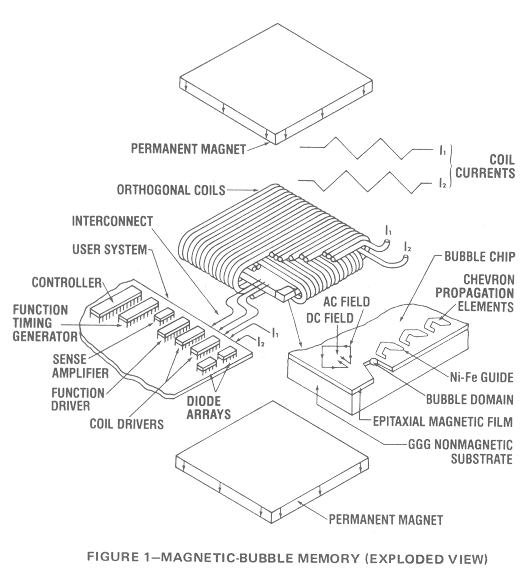
 The basic bubble-memory package contains the bubble-memory chip,
magnetic field coils, and permanent magnets as
shown in Figure 1. A rotating magnetic field created by two mutually
perpendicular coils causes the data in the form of
magnetic bubbles to move serially through the magnetic field in a manner
similar to data in a semiconductor shift register.
Two permanent magnets provide nonvolatility and allow for the stable
existence of magnetic-bubble domains.
Interfacing circuits that are compatible with standard TTL devices
complete the memory module to allow a convenient
building-block concept for the nonvolatile memory system.
The basic bubble-memory package contains the bubble-memory chip,
magnetic field coils, and permanent magnets as
shown in Figure 1. A rotating magnetic field created by two mutually
perpendicular coils causes the data in the form of
magnetic bubbles to move serially through the magnetic field in a manner
similar to data in a semiconductor shift register.
Two permanent magnets provide nonvolatility and allow for the stable
existence of magnetic-bubble domains.
Interfacing circuits that are compatible with standard TTL devices
complete the memory module to allow a convenient
building-block concept for the nonvolatile memory system.
The chip is composed of a nonmagnetic crystaline substrate upon which a
thin crystalline magnetic epitaxial film is
grown. Only certain materials exhibit the properties necessary to form
magnetic bubbles and these include orthoferrites,
hexagonal ferrites, synthetic garnets, and amorphous metal films.
Among these, the synthetic garnets have the best
combination of the desired properties. Synthetic garnets support the
formation of small magnetic bubbles that allow
high-density data storage. The bubbles are highly mobile and are stable
over a fairly wide range of temperatures.
The material chosen for the substrate depends on several factors. The
crystalline structure should be compatible with
that of the magnetic film, it should have nearly the same coefficient of
expansion, and it should be nonmagnetic. The most-used garnet substrate
with these properties is gadolinium gallium garnet (GGG). The magnetic
film grown on this
substrate has a crystalline structure that will allow the formation of
magnetic domains (bubbles) in a plane perpendicular to the substrate.
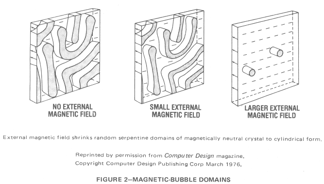
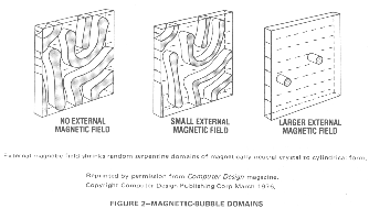 Without the influence of an external magnetic field, these magnetic
domains form random serpentine patterns of equal area,
minimizing the total magnetic energy of the magnetic film (see Figure
2). The magnetic field of the serpentine domains
tends to line up primarily along a single axis (the "easy" axis) that is
perpendicular to the plane of the film.
If an external magnetic field is applied, its energy tends to expand
domains polarized in the direction of the field and to shrink those
polarized
opposite to the field until they become small cylinders embedded in a background of opposite
magnetization. Viewed on end, these cylinders have the appearance of
small circles or bubbles with diameters from 2 to 30 micrometers.
Increasing the field further causes the bubble to collapse or to be
"annihilated". The external field
provides a bias that makes the bubbles stable. This bias, being a
static field, can be readily provided by permanent magnets with no
expenditure of power.
Without the influence of an external magnetic field, these magnetic
domains form random serpentine patterns of equal area,
minimizing the total magnetic energy of the magnetic film (see Figure
2). The magnetic field of the serpentine domains
tends to line up primarily along a single axis (the "easy" axis) that is
perpendicular to the plane of the film.
If an external magnetic field is applied, its energy tends to expand
domains polarized in the direction of the field and to shrink those
polarized
opposite to the field until they become small cylinders embedded in a background of opposite
magnetization. Viewed on end, these cylinders have the appearance of
small circles or bubbles with diameters from 2 to 30 micrometers.
Increasing the field further causes the bubble to collapse or to be
"annihilated". The external field
provides a bias that makes the bubbles stable. This bias, being a
static field, can be readily provided by permanent magnets with no
expenditure of power.
Before bubbles can be shifted through the magnetic film, they must be generated in accordance with input data.
Bubbles are generated by locally altering the bias field with a magnetic field produced by a pulse of current through a microscopic
one-turn metallized loop. This loop is located on a secondary layer immediately above the magnetic film on the surface
of the chip. Given a current of the correct amplitude and polarity through the one-turn loop, a localized vertical magnetic
field opposite to that of the permanent magnets is produced. This localized field establishes a domain wall inversion in
the magnetic film resulting in bubble creation.
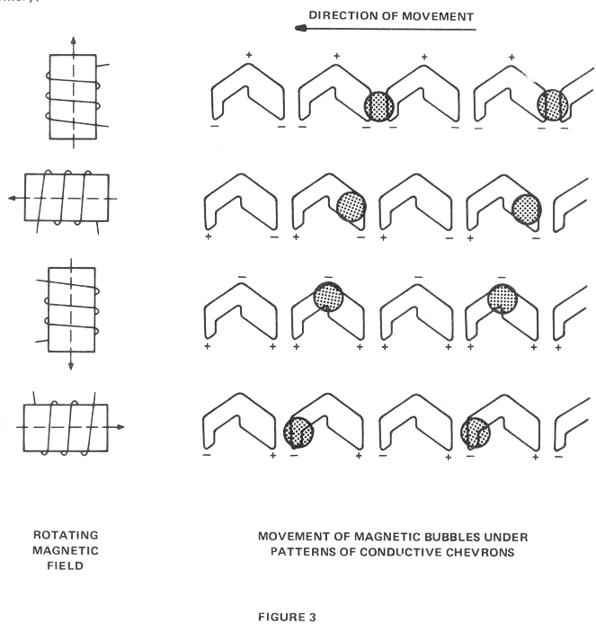
 Once a bubble has been created, a method is then required to move the bubble domain along a predetermined path.
This is accomplished by the deposition of chevron-shaped patterns of a soft magnetic material on the chip surface above
the magnetic epitaxial film. When magnetized sequentially by a magnetic field rotating in the same plane, these chevron
propagation patterns set up magnetic polarities that attract the bubble domain and establish motion. Figure 3 shows
the various polarities at different positions of the rotating magnetic
field. In actual practice the rotating in-plane magnetic
field is implemented by applying a two-phase alternating current to the two coils shown in Figure 1.
Once a bubble has been created, a method is then required to move the bubble domain along a predetermined path.
This is accomplished by the deposition of chevron-shaped patterns of a soft magnetic material on the chip surface above
the magnetic epitaxial film. When magnetized sequentially by a magnetic field rotating in the same plane, these chevron
propagation patterns set up magnetic polarities that attract the bubble domain and establish motion. Figure 3 shows
the various polarities at different positions of the rotating magnetic
field. In actual practice the rotating in-plane magnetic
field is implemented by applying a two-phase alternating current to the two coils shown in Figure 1.
|
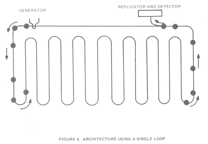
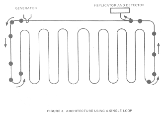 One possible implementation for the magnetic bubble memory is a long
shift register. As shown in Figure 4 the bubbles
would shift under the influence of the rotating magnetic field following
the path determined by the placement of
chevron patterns. Even though this approach offers the simplest design
and interface control, it suffers a major
disadvantage of having the slowest access time. The reason for this is
that after a data bit is entered or written it must
circulate through the entire shift register before it can be retrieved
or read. Another problem with this single loop design
is that a single fault in the shift register structure produces a
defective bubble memory chip. This results in a low
processing yield and a high cost to the consumer.
One possible implementation for the magnetic bubble memory is a long
shift register. As shown in Figure 4 the bubbles
would shift under the influence of the rotating magnetic field following
the path determined by the placement of
chevron patterns. Even though this approach offers the simplest design
and interface control, it suffers a major
disadvantage of having the slowest access time. The reason for this is
that after a data bit is entered or written it must
circulate through the entire shift register before it can be retrieved
or read. Another problem with this single loop design
is that a single fault in the shift register structure produces a
defective bubble memory chip. This results in a low
processing yield and a high cost to the consumer.
|
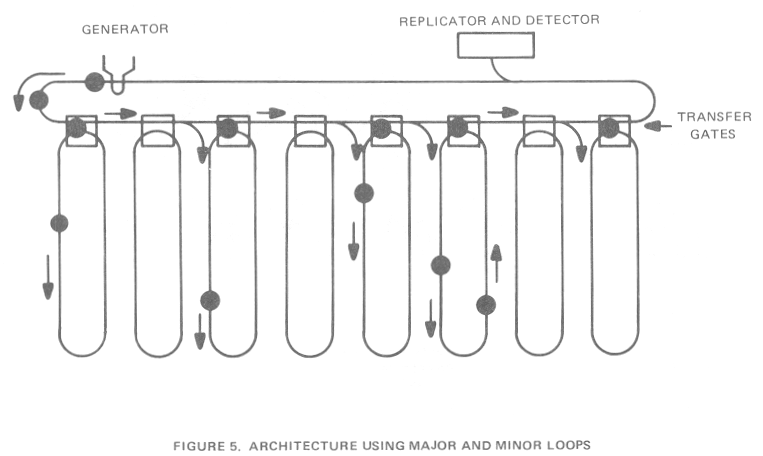
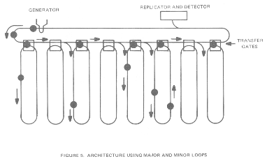 For these reasons TI has chosen the major-minor loop architecture, which offers a dramatic improvement in access time.
As shown in Figure 5, during a write operation (data entry), data is generated one bit at a time in the major loop.
The data is then transferred in parallel to the minor loops where it circulates until the next time data is to be read out of the memory.
For these reasons TI has chosen the major-minor loop architecture, which offers a dramatic improvement in access time.
As shown in Figure 5, during a write operation (data entry), data is generated one bit at a time in the major loop.
The data is then transferred in parallel to the minor loops where it circulates until the next time data is to be read out of the memory.
During a write operation data are introduced into the major loop by
pulses of current through the hairpin loop of the generator. The major
loop is essentially a unidirectional circular shift register from which
data can be transferred in
parallel to the minor loops. Thus a block of data is entered in the
major loop and shifted until the first data bit is aligned
with the most remote minor loop. At that time, each parallel transfer
element receives a current pulse that produces
a localized magnetic field causing the transfer of all the bubbles in
the major loop to the top bit position of the
corresponding minor loop. Once data is written into the magnetic bubble
memory, new data may be written only by
first removing the old data by doing a destructive read. In this
operation bubbles are transferred from the minor loops
and annihilated by running them into the Permalloy guard rail that
usually surrounds bubble devices.
During a read operation the data block to be accessed in the minor
loops is rotated until it is adjacent to the major loop. At this
time the data block is transferred in parallel to the major loop.
The block of data is them serially shifted to the replicator where the
data stream is duplicated. The duplicated data takes the path to the
magneto-resistive detector
element. The presence of a bubble in the detector lowers the resistance
resulting in a corresponding increase in detector current,
which can be detected via a sense amplifier. The original data stream
remaining in the major loop is rotated and transferred back into the
minor loops thus saving the data for further operations.
The magnetic-bubble-memory devices are fabricated using fine geometries
that make the manufacture of perfect
devices a difficult task. In order to increase production yields and
achieve correspondingly lower costs, redundant minor loops on the
bubble-memory chip allow some loops to be defective. Defective loops
are determined at final test and a
map of these loops is supplied to the end user so that the defective
loops can
be avoided in the final memory system.
This redundancy of minor loops can be handled in several ways. The map
could be written into a software program that
would direct data to be stored only to the perfect minor loops, but this
would require a unique software package for
each memory system. Alternatively, the map could be stored in the MBM
(magnetic-bubble memory) itself with some
risk of being written over with new data. The recommended approach is
to store the map in a programmable read-only
memory (PROM). Each bit in a page of data would then be written to the
MBM or read from it in accordance with the
contents of the PROM, thus preventing data bits from the defective minor
loops from mingling with valid data. Of course all this requires
control circuitry in addition to that necessary for the timing and
control of the alternating current in the field coils, the transfer of
data to and from the minor loops, and the replication and detection of
the magnetic bubbles.
interfacing with bubble memories
 Since the magnetic-bubble memory requires accurate current pulses for
the generate, replicate, and transfer operations,
an interface circuit called a function driver is needed to convert the
digital input control signals to the required current
pulses. Also, the two field coils each require a triangular current
drive 90 degrees out of phase with each other. This requirement is
satisfied with another set of interface circuits (coil drivers and diode
array) that is driven with digital input signals.
The output signal amplitude of the MBM is relatively small, about 3
millivolts. For this to be useful in a
system, the output is converted to standard TTL levels with the use of a
set of
interface circuits (RC networks and sense amplifiers). The block
diagram in Figure 6 shows the connection of all these interface circuits
as a memory module.
This modular building block promotes efficient construction of mass
memories.
Since the magnetic-bubble memory requires accurate current pulses for
the generate, replicate, and transfer operations,
an interface circuit called a function driver is needed to convert the
digital input control signals to the required current
pulses. Also, the two field coils each require a triangular current
drive 90 degrees out of phase with each other. This requirement is
satisfied with another set of interface circuits (coil drivers and diode
array) that is driven with digital input signals.
The output signal amplitude of the MBM is relatively small, about 3
millivolts. For this to be useful in a
system, the output is converted to standard TTL levels with the use of a
set of
interface circuits (RC networks and sense amplifiers). The block
diagram in Figure 6 shows the connection of all these interface circuits
as a memory module.
This modular building block promotes efficient construction of mass
memories.
|
|
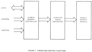
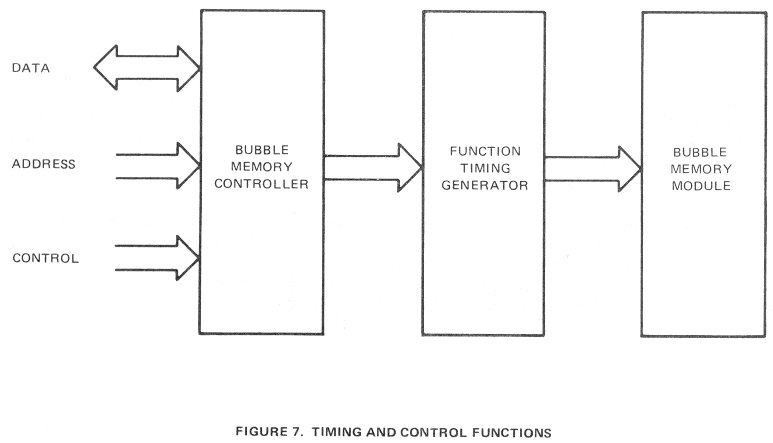
The control and timing signals for the memory module are derived from
the function-timing generator. This integrated
circuit provides input timing control to the function driver, coil
drivers, and sense amplifier on a per-cycle basis. The function-timing
generator provides control signals to the memory module as shown in
Figure 7. These signals provide control for five
basic operations: generate, replicate, annihilate, transfer-in, and
transfer-out. The function-timing
generator also initiates the rotating magnetic field and precisely
synchronizes the timing of other control signals with this field.
|
Figures 6 and 7.
The time at which a particular data bit is detected in the MBM may not
exactly match the time at which it is needed
in the system. The sense amplifier not only increases the voltage level
of the detected data, but also provides temporary
storage of the data bits in a circuit called a D-type flip-flop. The
sense amplifier receives a control input from the
function timing generator to transfer the detected data into the
internal flip-flop. In addition, the function-timing generator provides
the control signals necessary to put the existing data in a known
position during a power shut down. When the system is turned on again,
the stored data can then be accurately located and retrieved.
In a typical system the major computing and data processing is done by a
microprocessor. To provide a convenient
interface from the microprocessor to the MBM system, a custom controller
is needed for the read, write, and memory-addressing operations. The
TMS5502/TMS9916 MBM controller responds to commands from the
microprocessor system and sends control signals to the function timing
generator necessary to access a page (or pages) of data.
The controller maintains page-position information, handles
serial-parallel data conversion between the bubble
memory and the microprocessor, and generates the control signals to the
function-timing generator to perform read and write operations while
handling the redundancy of the minor loops.
advantages of bubble memories
The future growth of distributed process systems will be greatly
impacted by magnetic-bubble memories. These
microprocessor-based systems demand high-density mass storage at low
cost. Magnetic-bubble memories satisfy all of
these requirements with definite advantages over the existing magnetic
storage technologies. MBM's advantages over
moving-head disks or floppy disks are low access time (the time ncessary
to retrieve the desired data), small physical
size, low user entry cost, no maintenance, and higher reliability.
The advantages of MBM's over random-access memories (RAM's) are
nonvolatility, potentially lower price per bit,
and more bits per chip. The RAM has the advantage of much better access time, higher transfer rate, and simpler interfacing.
In summary, the main MBM advantages are the low entry price versus
disks for the low-end user, nonvolatility versus
semiconductor memories, and high-density storage in a small physical
space. Because magnetic bubble memories are a solid-state, nonvolatile
technology, they are ideally suited for portable applications as well
as providing memory for
traditional processing systems. Industrial applications include
memory for
numerical control machines and various types of process control.
Solid-state bubble memories are more reliable in harsh environments;
they are affected much less by shock, vibration, dirt, and dust than
electromechanical magnetic memories. Innovative new products include
data terminals, calculators, word processing, voice storage, and
measurement
equipment.
[END]
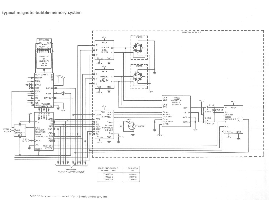
A typical bubble memory circuit,
from a datasheet later in the publication.

|
 The following text is taken from a Texas Instruments publication
entitled TIB0203 Magnetic-Bubble Memory and Associated Circuits
dated November 1978.
The following text is taken from a Texas Instruments publication
entitled TIB0203 Magnetic-Bubble Memory and Associated Circuits
dated November 1978.
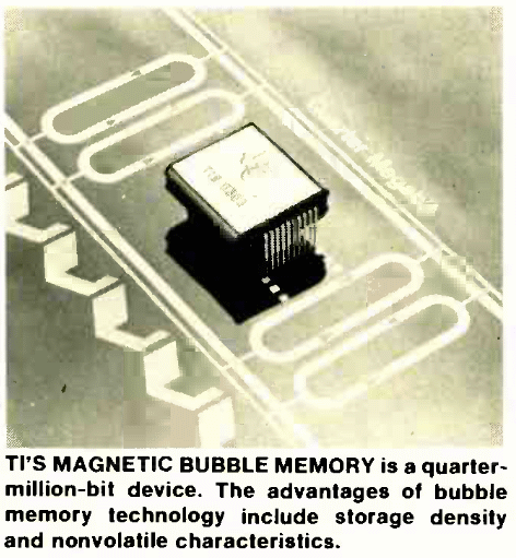 Some time in the last quarter of 1978, TI will release its new
quarter-million-bit magnetic bubble memory IC, the TIB0303, with a family
of interface and control circuits available in 1979.
Some time in the last quarter of 1978, TI will release its new
quarter-million-bit magnetic bubble memory IC, the TIB0303, with a family
of interface and control circuits available in 1979.