Interfaces were a central concern in our design of a microprocessor-based store-and-forward system at RCA, for international leased line communications.
We found it desirable to make a number of interface parameters program-selectable, or programmable. For example, in our communication link interfaces, transmission characteristics such as data rate, stop-bit length, character length, and parity are programmable and can all be set by simple software instructions.
Just how our design finally took shape will become evident as we present a description of the system's interface hardware and software.
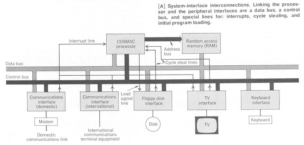
Figure A. (Click for a larger version.)
Moving messages through the system
Incoming messages enter the system through one of two communications interfaces. Here the messages are converted from a stream of bits into characters, each containing in an 8-bit data byte. These bytes are transferred, one at a time, into the system's semiconductor random access memory (RAM). When 232 bytes accumulate, they form a block of data.
The data block is then moved into the larger disk memory, where it is held until needed for retransmission. Outgoing data blocks move from disk, to RAM, to the appropriate communications line.
The RCA COSMAC microprocessor controls this sequence of events with programs written to fill the requirements of the overall store-and-forward communications process.
The entire microprocessor system (Fig. A) consists of a large-scale integrated microprocessor, a 4096-byte RAM, and five peripheral interfaces, each of which use a group of integrated circuit packages, and serve to connect different "devices" to the system.
The microprocessor makes both a data bus and a control bus available to the peripherals. These busses carry almost all the information that flows between the processor and the peripherals.
Since several different interfaces are connected to these busses, there must be a clear way to indicate which interface is permitted to be active at any given moment. The Select instruction performs this assignment function.
Each interface has its own, unique selection number. For example, a Select instruction together with the number 08 on the data bus, will activate the floppy disk interface. Once an interface is selected, it is free to act on further processor instructions.
To control certain peripheral functions - such as disk startup and head location, or communications transmission speed - the processor issues a Set instruction. Other processor instructions are used to test the state of external flag lines. These lines are connected to flip-flops, set by the peripheral interfaces to indicate such conditions as readiness to read or write, as well as faults and error conditions.
Three special lines allow the peripheral interfaces to initiate system actions, without first getting permission from the processor. By using the Interrupt line, the communication interfaces demand immediate handling of incoming data as it arrives on the communications links, and an immediate supply of outgoing data from the RAM, as it is needed for transmission over the links. With the Cycle steal lines, the floppy disk memory and TV display gain direct access to the RAM so they can write into the memory, or read from it, without software instructions. Finally, via the Load line, the system can be reset and restarted - using a disk-stored program - after a catastrophic failure or loss of power.
Inside the communications interface
When a communications interface has received an incoming character from its communications link, it raises the microprocessor interrupt line. At the same time, this unit raises an external flag, EF1, to indicate that a received character is available.
At the microprocessor, the interrupt causes the ongoing program to branch to a special software routine designed to service interrupts. Since there is only one interrupt line, the routine must first find out which is the two communications interfaces sent the interrupt, and then determine what kind of service is needed. This information is obtained by testing to see which external flags are raised.
The actual programmed sequence in the interrupt routine includes a Select instruction for each communications interface. After an interface is selected, its external flags are tested to determine the presence and cause of the pending interrupt. Knowing the device and its flagged condition, the processor issues an appropriate instruction to service that condition. For example, in response to flag EF1, indicating a received byte of data is available, a Read instruction would be issued to call for the transfer of a byte of data from the communications interface to the procesor (for transfers in the opposite direction, a Write instruction is used). On receipt of the Read instruction, the interface places the received byte on the ingoing data bus, and the processor clocks the byte into RAM memory.
The system allows up to four external flags (EFs) for each peripheral interface, and the meaning of each of these flags - or combinations of flags - can be different for each interface. For the communications interfaces, EF4 is set in conjunction with EF1 if the received character is erroneous (bad parity). When an interface is transmitting data, EF2 is set to indicate that the next character can be transferred. Finally, EF3 is used to indicate special conditions, such as abnormal communcation line operation.
While a given interrupt is being serviced, all other interrupts must wait their turn. Priorities for servicing interrupts are established in the processor's software interrupt routine. For example, the domestic communications interface is always selected first by the routine. Domestic data rates are usually higher then international rates, and therefore the penalty for keeping the domestic line waiting is greater. Likewise, Read interrupts are always given priority over Write interrupts, because failure to read may result in loss of data, but the worst penalty for failure to write is time lost on an idle transmission line.
The interrupt-driven form of data transfer is well suited to the communications function. Competing functions and devices are easily queued; each input character can be examined and processed as it is received; new devices are easily added; and existing device priorities are easily changed.
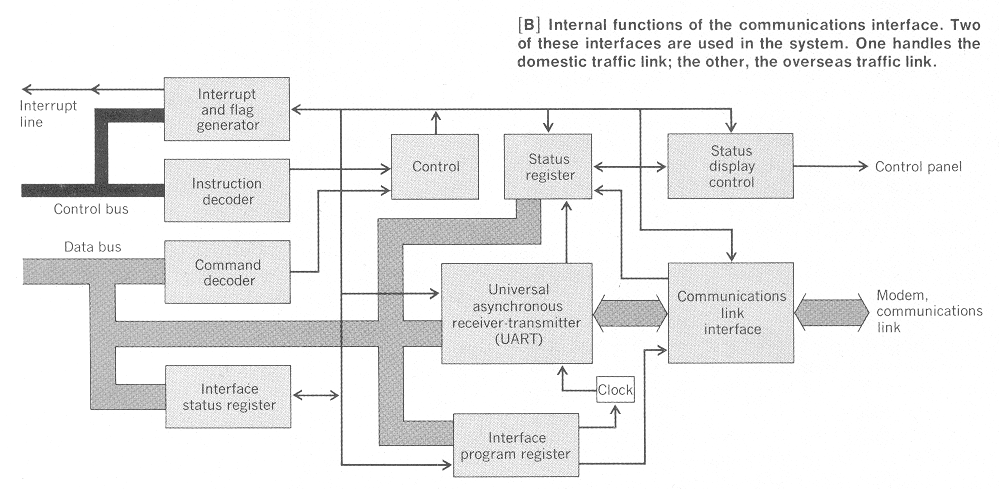
Figure B. (Click for a larger version.)
The hardware that communicates
Communications interface hardware centers on a large-scale integrated circuit - contained in a single 40-lead package - that handles several key functions. This circuit, called a Universal asynchronous receiver-transmitter (UART), converts data bytes from the microprocessor into a stream of serial bits for the communications link. The UART also performs the opposite conversion, taking serial bits from the communications link and shaping them into characters for the microcomputer system. Actually, each character consists of up to 8 data bits, and an odd-even parity bit may be added. When called for, these parity bits are generated by the UART as it transmits characters, and the UART also checks the parity of incoming characters from the communications link.
Surrounding the UART are a number of functional blocks implemented in transistor-transistor logic (see Figure B). The Interface program register provides the means for microcomputer program instructions to control the Clock and the communications mode (half- or full-duplex). Flip-flops in this register select speed-control lines into the clock to allow program selection of bit-per-second transmission and reception rates. The type of parity (even or odd), length of characters, and number of stop bits used in serial transmission are also under program control.
To connect the transistor-transistor logic (TTL) circuits in the interface to communications link circuits, some matching is necessary. This is done in the Communications link interface circuitry. For links using RS-232 industry-standard data interfaces, voltage-level shifting of TTL signals is needed. For teletype links, output currents must be controlled to specified levels. Some communications links require that there be no direct ground connections. For these, optical isolation devices must also be included.
Instructions to the communications interface from the processor are received over the system's control bus and routed through the Instruction decoder which interprets microprocessor codes and generates logic signals that can be used to control the interface hardware. Since some of these microprocessor codes come over the system data bus, there is a Command decoder to interpret this added information. The Interface status register indicates whether the interface is, or is not, currently selected and thus allowed to communicate with the processor.
The Control logic distributes all the appropriate information to the Interface program register, the UART, and other parts of the interface. The external flags that inform the processor of the interface current status are placed on the system's control bus by the Interrupt and flag generator. This information comes from the UART and Status register, which is used by the UART and other circuits to record the occurence of such fault conditions as parity errors and open communications lines.
The third major element of the system, in addition to the communications interface and the microprocessor-RAM combination, is the floppy disk interface.
Stealing cycles for more efficient operation
The key feature of the floppy disk interface is its direct access to RAM memory, without need for detailed microcomputer program control. Using this direct memory access feature - built into the COSMAC processor - the disk can put data bytes into the RAM, or take them out, without receiving even a Select command. In fact, it can transfer this data while the processor is occupied with other tasks, such as talking to a communications interface.
The direct memory access mechanism used here is called cyycle stealing. There are normally two microprocessor cycles for each program instruction: a fetch cycle, followed by an execute cycle. When the cycle steal line comes up, say during a fetch, the processor will complete that fetch, and the corresponding execute cycle, and then hold its breath for a one-cycle interval before moving on with the next instruction, fetch cycle. It is during these stolen one-cycle intervals that data bytes are moved between the RAM and the disk.
Before the cycle stealing can begin, a direct memory access address register must be loaded with the first RAM memory address of the data block to be read from, or written on, the disk. Then the register is automatically incremented at each succeeding stolen cycle, until an dentire block of 232 data bytes has been transferred. And all the processor sees is a slight slowdown, usually less than a 1-percent reduction in the time available for its ongoing program activities.
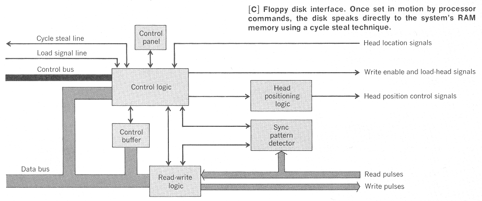
Figure C. (Click for a larger version.)
Controlling the floppy disk
The floppy disks used in this system are 7.5 inches in diameter. Data is recorded on one side of the disk - coated with oxide material - which is made of flexible plastic. The disk is packeted in a paper envelope, and a recording band, about one inch wide is accessible through the envelope.
During reading and writing the disk is "loaded," so that physical contact is made between the read-write head and the disk surface. Since this causes wear, it is desirable to unload the disk as soon as possible. The disk rotates at 90 r/min, can store 1.4 Mb, and costs about $5. Data can be transferred from the disk at a rate of 33 kb/s, and it tkaes an average of 560 ms to reach a desired specific data block on the disk.
Each of the disk's 64 concentric data tracks can hold 8 complete blocks of data. And each of these blocks begins with 16 bytes of synchronization information, followed by 232 bytes of data, and capped off by 8 bytes of trailing zeros.
This structure provides an 11-ms gap between adjacent blocks on the same track, and this gives the system enough time to process the blocks one right after another.
Data from the disk is always transferred to the system's RAM memory, before going elsewhere, and all data stored on the disk comes to it from the RAM.
As with the communications interfaces, a Select instruction - including the disk's identifying number - is used to initiate contact between the processor and the disk. Four additional instructions are used to control disk functions. Locate A and Locate B specify the disk storage location for each block of data; Start loads the disk head and allows data flow to or from the disk when the desired location is reached; Stop unloads the disk when the desired data transfer is completed.
To follow these disk control operations in more detail, refer to the interface function diagram in Figure C. The Locate A instruction sends the desired track-location number to the interface Control Logic, and Locate B sends the corresponding sector-location number.
Actually, the Locate B instruction serves a double purpose since it also tells the control logic whether data is to be written onto the disk or read from it. This information, along with the current track and sector location data, is stored in the Control Buffer, where it is available until updated by new Locate A or Locate B instructions.
When a Start instruction is received, the Control Logic activates the Head Positioning Logic to move the head into the position stored in the Control Buffer, and simultaneously loads the head into contact with the disk.
After the disk mechanisms have had time to settle to steady-state operation (delays to guarantee this are generated by the Control Logic), the actual data transfer is initiated by the interface itself. No processor instructions are needed during this transfer, which is not complete until an entire block of data has been moved.
When the disk is to be read, the disk head is first loaded, the desired location is reached, and the read circuits are activated somewhere within the 16-byte synchronizing pattern that prefaces the desired block of 232 data bytes. The Sync Pattern Detector then searches for the synchronizing pattern to determine the exact moment when the first data bit in the block is about to move into position under the read-write head. This mode of operation allows large design tolerances on both the location of the head and on the timing for reading and writing.
The Read-Write Logic frames the data bytes while the disk is read. That is, it defines the beginning and end of each byte as it appears in the serial stream of one-bit read pulses from the disk. When it is time to transfer a byte of data to microcomputer RAM, the Control Logic raises one of the cycle steal lines, and the byte is then placed on the system data bus. When data is being recorded on the disk, the Read-Write Logic takes in each data byte and converts it into a stream of one-bit write pulses to the disk head.
At the present time, the Read-Write Logic adds a parity bit after every 8 bits it sends to the disk. When the disk is read, these parity bits are checked to get indications of errors that may have occurred during the disk read operation. Since disk errors tend to occur in bunches, or bursts, future system design plans plans call for the use of burst error-detecting coding techniques rather than parity bits. The savings in available storage space should be substantial.
In addition to coordinating all the other disk interface operations, the Control Logic sets the external flags that notify the processor about disk conditions. For example, a flag is raised when the interface finishes transferring a complete block of data to the RAM, or when a complete block of data has been written on the disk. By testing this flag, the microprocessor program can decide when to change Locate instructions, and initiate new Start instructions to read or write additional data blocks.
As a convenience feature, the disk stores a bootstrap program that can restart the entire microcomputer system from scratch after power is lost, or after some other unanticipated condition puts the system out of commission. Any other program residing on the disk can then be loaded using the bootstrap program, eliminating the need for auxiliary program load devices such as cassettes or paper tape, and greatly simplifying system regeneration after a crash.
Less vital to the system than the floppy disk, but still interesting from an interfacing viewpoint, is the TV display.
Talking to a TV display
The TV can display text indicating communication-link fault conditions. But experience has shown that its most useful function is to display memory patterns; bit patterns on the data bus; and other information for diagnosis, test, and maintenance of the system.
A standard, unmodified TV set is used for the display which is refreshed from 128 bytes of RAM memory. This storage space is dedicated to the display, and these data provide 1024 dots for the display. Like the floppy disk, the TV display uses the direct memory access (cycle-stealing) capability of the system.
Every 60th of a second, the TV interface interrupts the processor and asks for new information. The interrupt routine then points to the beginning of the 128 bytes of RAM memory that contain the TV display data. These data are then sent to the TV interface on a cycle-stealing basis.
Since only one peripheral device can be served at a time by the direct memory access capability, the disk and the TV cannot operate simultaneously. The disk, vital to the main communcations function of the system, is given absolute priority over the TV. The result is that when disk and TV needs conflict, the TV display may flicker or show a reset pattern for up to about 1/2 second.
The lowest-priority peripheral in the system is the manual keyboard used to enter data butes (in the hexadecimal code internally used by the system) into the RAM memory. This provides a means to debug and modify programs - for example, to change track and sector numbers manually for floppy disk operations.
Paul M. Russo (M) joined RCA Laboratories, Princeton, N.J., in September 1970. There, he has done research in the areas of computer architecture, program behavior, computer system performance evaluation, microprocessors, and data communications. During the 1969-70 academic year, he taught circuit theory and circuit optimization at the University of California, Berkeley. Dr. Russo was born in Plevlje, Yugoslavia, in 1943. He received the B.Eng. degree in Engineering Physics from McGill University in 1965, and the M.S. and Ph.D. degrees in electrical engineering from the University of California, Berkeley, in 1966 and 1970. He is a member of ACM, Eta Kappa Nu, and Sigma Xi.Michael D. Lippman (M) has been a member of the Technical Staff of the RCA Laboratories, Princeton, N.J., since 1966. He has done research on magnetic data recording, vapor transport processes, and graphics development and design of microprocessor-based data communications systems. Mr. Lippman is a member of Tau Beta Pi and Eta Kappa Nu.